
PCB fabrication Process 18
[otw_is sidebar=otw-sidebar-1]I hope you are doing good, in the previous series of tutorials I have discussed the PCB designing staircase and application of popular PCB design software at beginners’ level for designing the PCBs. In this article I will discuss the complete fabrication process. That is how the PCB manufactured physically.
After reading this article the reader will be able to learn about different steps involved in PCB Fabrication Process. So sit back, keep reading and enjoy learning.
After the PCB is designed the softwares generate the Gerber files which are sent to the PCB fabrication house for manufacturing.
PCB fabrication Process:
The steps involved in the PCB fabrication are:
-
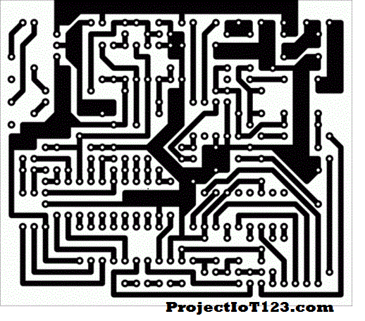
Printing the Photoplot:
The PCB layout is first of all printed on the transparent sheet. Thus the Photoplot will consist of two portions: the portion in white and the portion in black. The Photoplot is as shown in the following image:
-
Coating the Laminate with Photoresist
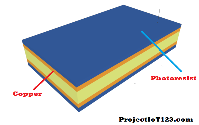
Laminate:
Laminate is the FR4 fibre glass with copper pre bonded on both sides of the board.
Photoresist:
Photoresist is the photosensitive dry film which is coated on to the Laminate in order to print desired copper pattern.
So the second step is to coat the dry film of the photosensitive material onto the copper sheet.
-
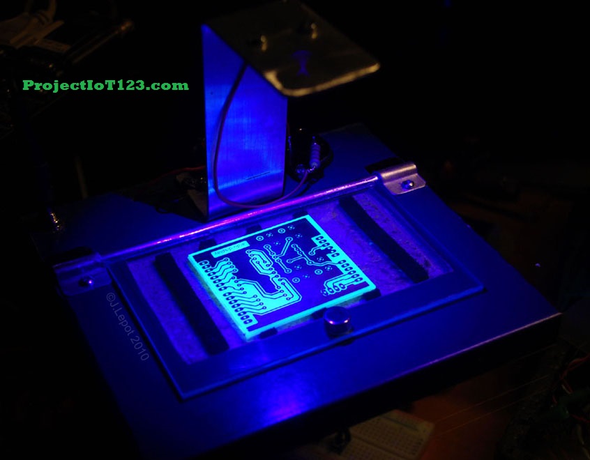
UV light Exposure
After these two processes the copper board coated with photoresist is sandwiched between the Photoplot and the UV rays are blasted on it. The black portion of the Photoplot will block the UV light and thus the photoresist remains as it is and the transparent portion is exposed to UV rays due to which the photoresist becomes hardened.
-
Removing the Unhardened Photoresist
Now the unhardened portion of the photoresist which is not exposed to UV rays is removed by washing the copper board with the alkali solution. Thus in this way the photoresist will only remain coated on the desired portion of copper.
-
Etching the Copper
Now it’s time get rid of the extra copper. The copper board is now washed with the strong alkali solution in order to etch away the unwanted copper. Those portions of the copper board which are not covered by the hardened photoresist will dissolve or etch away in the alkali solution; on the other hand the copper below the hardened photoresist will remain intact as it is not exposed to alkali solution. It is shown in the following figure:

-
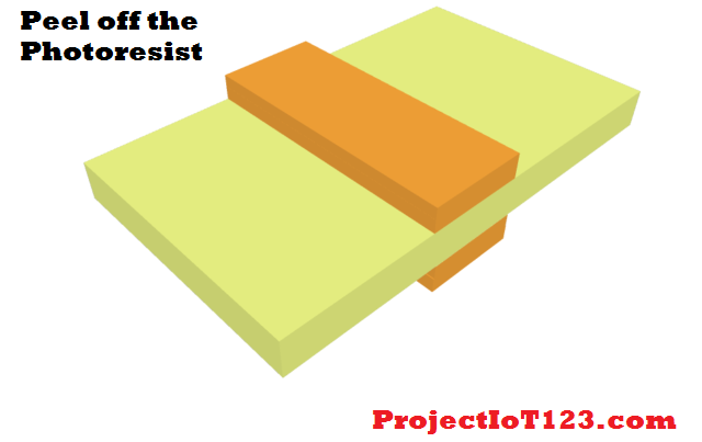
Peel off the Photoresist
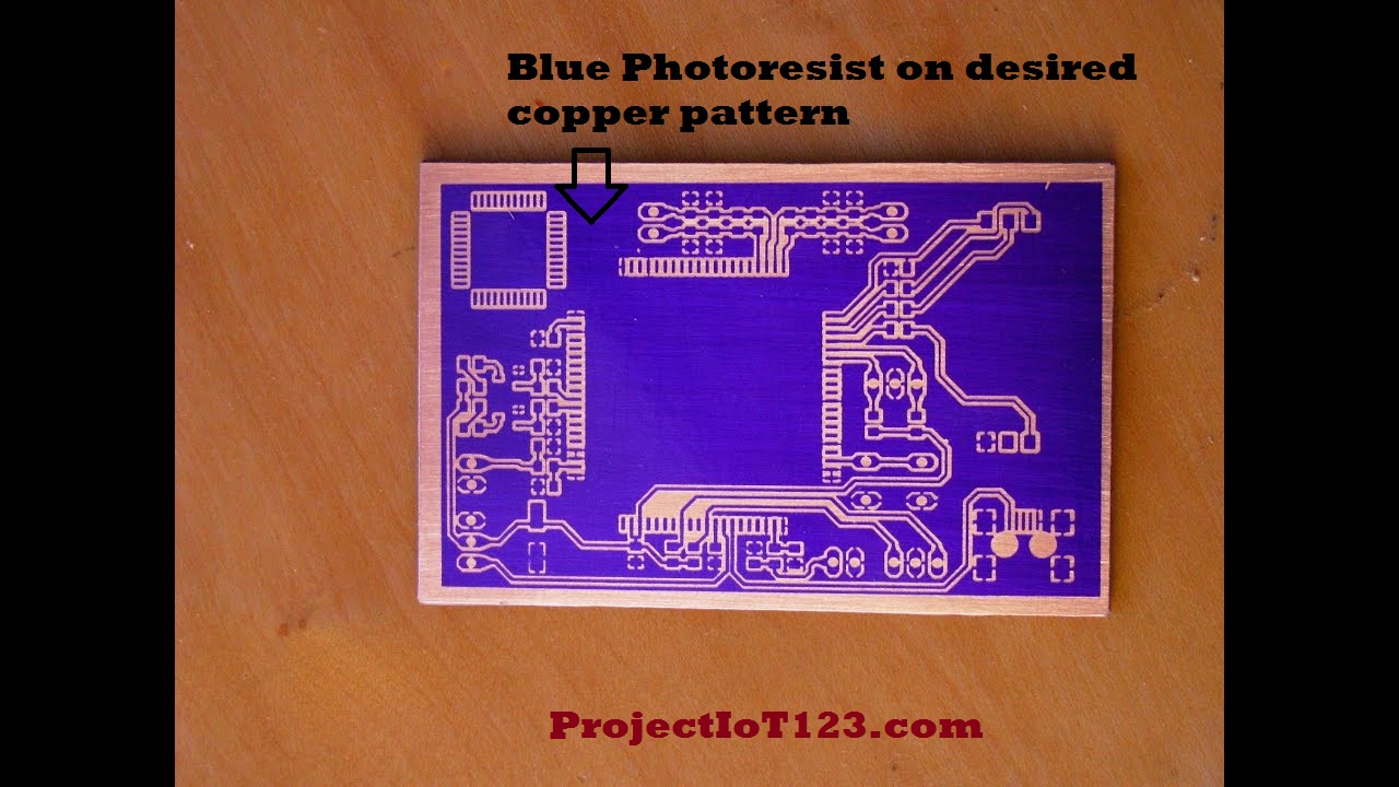
Now peel off the photoresist to reveal the desired copper pattern underneath. It is shown in the following image:
-
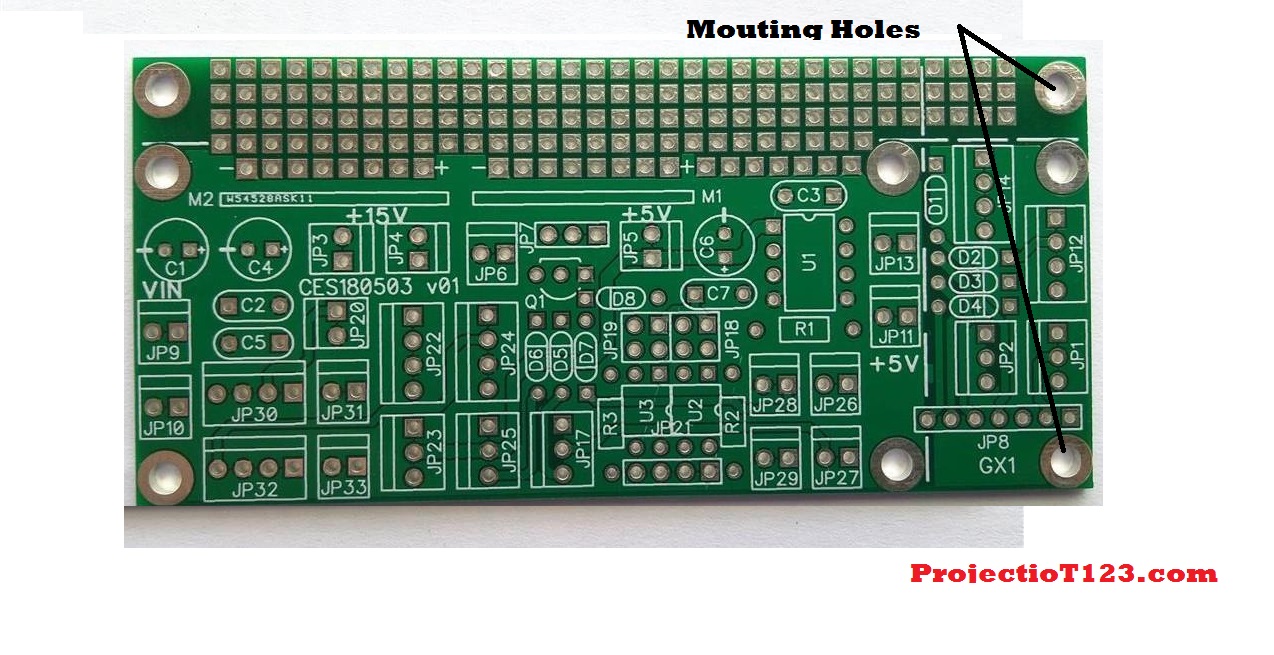
Drilling
The next step in the PCB fabrication is drilling holes in the copper board. There are three types of holes drilled into the printed circuit board.
Mounting Holes:
Mounting holes are drilled on the PCB according to layout guidelines. The mounting holes are used to mount on anything with the help of screws:
Through Holes:
Another type of holes drilled into the PCB is the through holes which are used for placing the electronic components on to the printed circuit board.
Vias:
The most important hole present on the PCB is the via. With the help of this hole the connection is established from top layer to any other layer.
In the most basic layer only the mounting holes and through holes are drilled. Thus in this way the board is ready and then electronic components either discrete or integrated circuits are assembled onto the board.
That is all for now, I hope this tutorial would be helpful for you. In the next tutorial I will come up with another important topic on engineering. Till then stay connected, keep reading and enjoy learning.
NICE POST
HI I AM NEW IN ELECTRONICS
PLZ TELL ME CHEAP PCB MAKER
hello
you need pcb maker or pcb designer ?
email me at microsolutionpk2@gmail.com
camisetas de futbol baratas
camiseta atletico de madrid 2024
Thank you for your sharing. I am worried that I lack creative ideas. It is your article that makes me full of hope. Thank you. But, I have a question, can you help me?
camiseta arsenal 2024
mail order pharmacy india http://indiaph24.store/# buy prescription drugs from india
mail order pharmacy india
mexico drug stores pharmacies: Online Pharmacies in Mexico – medicine in mexico pharmacies
reputable canadian online pharmacy canadian pharmacies recommended canadian pharmacies
http://mexicoph24.life/# buying from online mexican pharmacy
india pharmacy mail order https://indiaph24.store/# Online medicine home delivery
reputable indian pharmacies
mexican mail order pharmacies mexican pharmacy mexico pharmacies prescription drugs
http://lisinopril.network/# buy zestoretic
zestril 20 mg lisinopril 5mg prices zestril 2.5 mg
cost of generic propecia: cost propecia online – order generic propecia price
buy ciprofloxacin over the counter ciprofloxacin generic ciprofloxacin order online
https://ciprofloxacin.tech/# ciprofloxacin mail online