
Introduction to EasyEDA PCB Tutorial 19
[otw_is sidebar=otw-sidebar-1] I hope you all are doing good, in the previous tutorial I have discussed about the PCB design staircase, I have also discussed popular PCB design softwares and basic commands employed to develop the layout at the beginners’ level.
I am starting another series of tutorials in which I will discuss PCB design in EasyEDA software. EasyEDA is a popular software used for circuit simulation, schematic development and PCB designing. After reading this tutorial the reader will be able to learn about the PCB design technique and User Interface of the EasyEDA software.
EasyEDA Library:
Before starting it is important to note that the PCB design methodology is almost the same in all PCB design softwares. The only thing that varies from software to software is how handy its User Interface is and how much it offers its users to design the PCB.
Some of you must have used some kind of circuit simulator in order to assess the working of the circuit prior to its real world realization thus you must have noticed that in order for the software to run the simulation it is important that the simulation models of all the electronic components employed in the circuit is present in the library of the software.
Introduction to EasyEDA PCB Tutorial:
Similar is the case for PCB designing. Before the PCB designer start developing the PCB the first step is to make the footprints of the electronic components. If the footprint of an electronic component that is to be employed in the circuit is not present in the library of the software the software will could not design the PCB. Fortunately footprints of most of the components are already installed in the library of the softwares so one can readily use them. But if it is not present then the first step in developing the PCB is footprint designing. EasyEDA has a rich library of footprints and it is quite handy to use.
I have already discussed the PCB design methodology in detail in my previous tutorials where I have explained each step in detail.
EasyEDA User Interface:
Before you start developing the layout of your circuit its schematics and footprints of all the components should be available in the EasyEDA software.
The user interface of the EasyEDA is as shown in the following image;
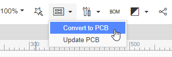
After you have successfully developed the schematics convert the schematics into the PCB. Remember that the schematics will only get converted into the PCB if all the footprints are present in the library of the EasyEDA PCB library. Convert the schematics into the PCB as shown in the following figure:
The design area will open in which all of the components’ footprints will be placed randomly. So the next step is to properly arrange all of the footprints. The footprints are placed according to the placement guidelines or the guidelines provided by the client.
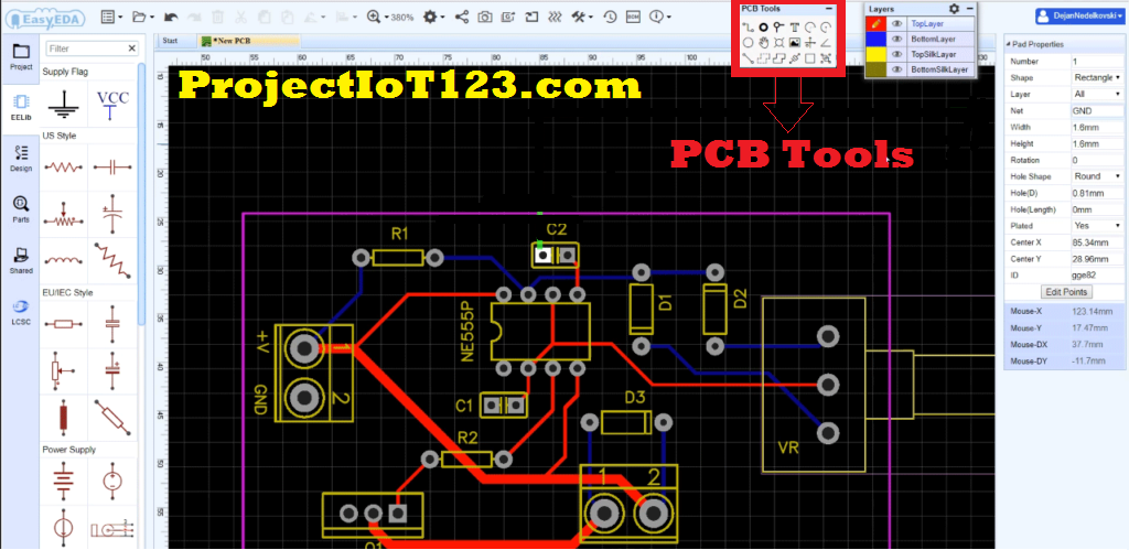
The PCB tools employed most frequently for PCB designing are presented at the top of the User Interface as shown in the following image:
At the right side is the layers toolbar in which the list of all the layers employed in the PCB are listed as shown in the following image:
The detailed discussion on layers is made in my previous tutorials. It is recommended to go through my previous tutorials if you do not know about the layers in the PCB.(Introduction to EasyEDA PCB Tutorial)
That is all for now I hope this tutorial would be helpful for you. In the next tutorial I would come up with more interesting topics of engineering. Till then stay connected, keep reading and enjoy learning.