
pcb design altium tutorial 1
I hope you all are fine, in the previous series of tutorials I have discussed the PCB design stairway in EasyEDA and have briefly explained the basic tools and commands employed at the beginners’ level for designing the PCB.
After reading this tutorial the reader will be able to learn about the User Interface (UI) of the Altium and the stairway of designing the PCB in Altium. So sit back, keep reading and enjoy learning.
PCB Design Stairway in Altium:
As we commence start learning the PCB design there are some points that should be addressed first. First point is, the PCB design methodology is same in all softwares, and the only difference between the softwares is the User Interface of the software and the available commands that let the PCB designer work more efficiently. Some of the advanced PCB design softwares has quite handy UI and provide the user a lot of features that eases the designer in his / her design venture Altium is one of the softwares that is used by professionals at advance level.
pcb design altium tutorial:
Second is the PCB design process. As discussed in previous series that the schematic symbol that is used to be in the schematic design should be present in the library of the software before one can use it and the simulation model of the component whose simulation is to be carried out should be present in the library of the software, similarly the footprint of the component that is used in PCD designing should be present in the library of the Altium. So the PCB design staircase starts with footprint development.
Footprint in Altium:
Footprint can be defined as the pad on which the component is mounted and soldered. If the footprint of the electronic component that is deployed in the circuit is not present in the library of the Altium then the footprint designer has to design the footprint first.
Placement in Altium:
One of the perks that make Altium popular among the PCB designer is the ease that it provides to its users. As soon as the circuit engineer start drawing the schematics of the circuit the footprints of the electronic automatically appear in the PCB design area with the connections shown by the rats. The PCB designer then has to organize those footprints. The footprints are placed according to the guidelines provided by the client or the PCB design engineer himself / herself exploits expertise.
Board Outline in Altium:
After the placement has been done successfully next the PCB designer defines the board outline according to the guidelines.
Routing in Altium:
Routing is the final and most time consuming task in PCB designing in which the copper is drawn from one pin of the electronic component to the next pin of the electronic component. Various commands that aid the designer are presented to the user for routing. There are a number of design constraints that are to be considered while routing the printed circuit board. Some of the considerations for routing are bent angle of the wires, width of copper etches, air space between two adjacent copper routes, placement of vias and many more.
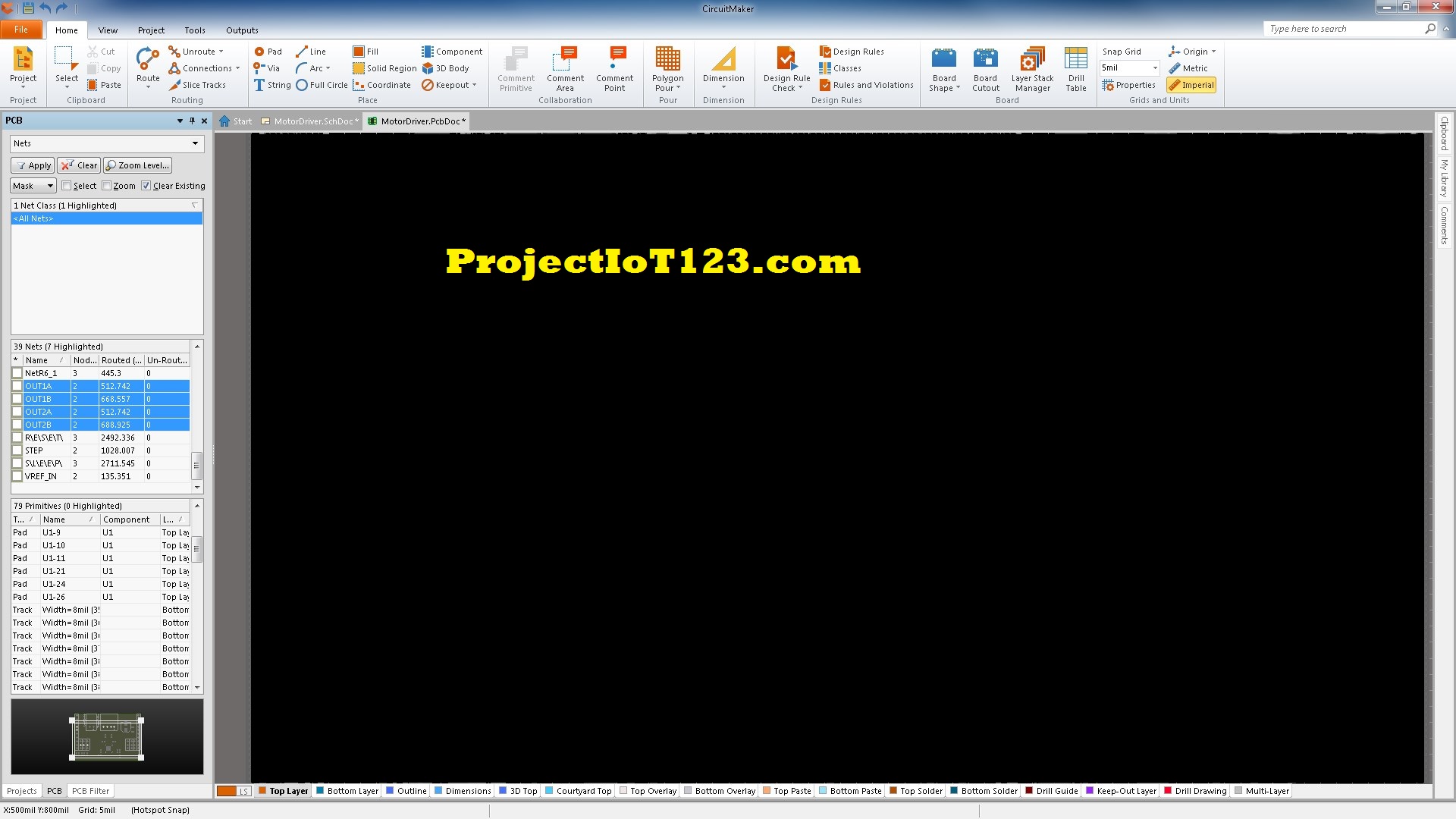
Altium User Interface:
The Graphical User Interface of the Altium PCB designer is as shown in the following image:
That is all for now, I hope this tutorial would be helpful for you. In the next tutorial I will discuss some of the common tools and commands that are used at the beginners’ level for developing the layout of the printed circuit board. Till then stay connected, keep reading and enjoy learning.s
what a great post