

zener diode as voltage regulator 2
[otw_is sidebar=otw-sidebar-1]
In this article I will discuss one of the most important electronic components i.e. Zener Diode. At the end of this article you will be able to learn about.
- What is the Zener Diode?
- V-I characteristics of Zener Diode?
- Construction and Working of Zener Diode?
- Applications of Zener Diode?
- zener diode as voltage regulator
So keep reading and enjoy learning.
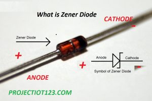
What is Zener Diode?
[otw_is sidebar=otw-sidebar-3]
A zener diode is just like a simple p-n diode except with one difference which let it do a number of useful feats that a simple p-n diode can not do. First let discuss what is the Zener diode then I will come to that difference.
A zener diode is just like the normal p-n diode in the forward bias and has exactly the same V-I characteristic as that off normal p-n diode.
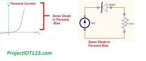
As you can see in the picture forward characteristics of the Zener Diode is exactly similar to that of the normal p-n diode. The difference lies in the Reverse characteristics of the Zener Diode. The important feature of the Zener Diode which makes it so useful, is their ability to work in the reverse bias. Unlike normal p-n diode the Zener diode can withstand the reverse biasing due to which it finds applications of practical interests for example Zener Diode can be used in
- Voltage Reference.
- Voltage Regulator.
Let’s now disscuss how the Zener Diode is able to withstand the Reverse Biasing.
[otw_is sidebar=otw-sidebar-3]
Construction and Working of the Zener Diode:
The Zener Diode is optimized to work in the Reverse bias. The contruction is similar to that of the normal p-n diode except that Zener diode is doped heavily as compared to that of the normal p-n diode which gives rise to the ZENER EFFECT. The Zener Effect is named after Clarence Melvin Zener who discovered this effect. This phenomenon makes Zener diode to bear the reverse breakdown in contrast to the normal diode which gets destroy in reverse bias.
Due to heavy doping in the Zener Diode a phenomenon of tunneling occurs. The heavy doping of the zener diode makes the depletion region very thin so that when electric field is applied to the diode in reverse direction it ruptures the depletion region and a phenomenon results which called Quantum Tunneling. Quantum tunneling is out of the scope of this article. In short due to this Quantum Tunneling Zener Breakdown occurs in the reverse bias of the Zener Diode which is a controlled breakdown and does not destroy the Zener Diode. The Zener Effect is dominant in the Zener Diode at or below 5.6 volts and Avalanche Breakown is dominant above 5.6 volts.
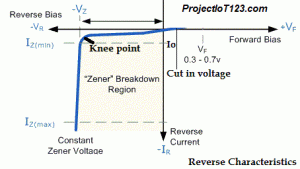
Let’s discuss now the V-I caharacteristics in the reverse bias.
As can be seen in the image above at the Knee point the the current increases instantaneously and we need a current limiting resistor to control the current to keep it in the allowable limit of the Zener Diode. The voltage at which the Zener Breakdwon occurs is called the Zener Voltage. This operating point is very impotant in many applications.
[otw_is sidebar=otw-sidebar-2]
Applications of the Zener Diode:
Due to the ability of the Zener Diode to work in the Reverse bias it founds applications in the Voltage Reference circuit and also can be used as the voltage regulator. Let’s first disscuss the Voltage Reference.
Voltage Reference :
A voltage reference circuit is used to generate the constant voltage which is used as a reference voltage and is independent of the loading of the circuit and the power supply variations. The Voltage Reference can be used in power supplies, Analog-to-Digital Converter, Digital-to-Analog Converter and many other useful applcations. So a Zener can be used in this applications and can provide accurate and stable voltage reference. The sharp knee in the V-I characteristics of the Zener diode enables it to provide a stable and voltage indpendent voltage reference.
Due to the steep curve in the V-I characteristics the large change in the input voltage causes very low change in the output of the Zener Diode which is also due to its low resistance in the Reverse Direction. So a Zener Diode is important in voltage reference circuit.
zener diode as Voltage Regulator:
A zener diode can be used to provide the stabilized output voltage despite of the variation in the input voltage. As the voltage above or equal to the Zener breakdown of the Zener Diode is applied across the Zener Diode in the reverse direction the Zener Breakdown of the diode occurs and output of the Zener diode becomes equal to what Zener Diode is designed to provide. For example a 3.6V volt Zener Diode has breakdown voltage at 3.6V i.e. when voltage equal to or greater than the breakdown voltage(3.6V) is applied across the Zener Diode in reverse direction the Zener Breakdown occurs and the output voltage of the Zener Diode becomes fixed at 3.6V. This is due to the steep curve of the V-I characterisics of the Zener diode and low resistance in the Reverse breakdown. The following circuit shows the way Zener Diode can be used as the Voltage Regulator.
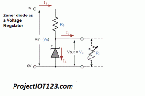
As can be seen in the circuit above the Zener Diode is connected in parallel to the load to provide the stabilized voltage across it. And also note that the Zener diode is connected to the current limiting resistor Rs so that the Zener diode can be properly biased and the power supply can not burn out the diode.
As the input voltage varies the voltage the input current also Is also varies but the voltage across the Zener diode remains constant as it has low resistance in the Reverse Breakdown which results in very low change in output vooltage corresponding to the large change in input current or input voltage. In this way the Zener diode can be used to stabilize the voltage across the load and serves the important task of the Voltage Regulaion.