
PCB Design in Proteus 3
[otw_is sidebar=otw-sidebar-1]In this post I will take you through (PCB Design in Proteus)process of designing the printed circuit board in Proteus. If you are an electronics engineer then you should have the skills from the schematic design to the printed circuit board design. There are a lot tools for designing the printed circuit board but the most common and easiest is the Proteus. The Proteus is very popular among the professionals and students because of its large number of capabilities. The Proteus software can be used for schematics drawing, simulation of circuits, printed circuit board design and three dimensional visualization of the printed circuit board. [otw_is sidebar=otw-sidebar-2] After reading this post you will be able to learn the schematic drawing in Proteus and the designing of the printed circuit board in the Proteus, you will also learn about how to visualize the three dimensional view of the circuit in Proteus. So sit back, keep reading and enjoy learning.
What is Proteus?
Proteus is the circuit simulation software and can also be used for printed circuit board design. Proteus can also be used as the development tool in which you can write and simulate the code on any microcontroller.
Proteus Library of Components:
In order to draw the schematic in the any circuit simulation software you need the library which holds the symbol of the component to be used in the schematic. The symbol of the component to be used in the schematic must be available in the library of the software for schematic drawing, in the similar way the simulation model of the specific component to be placed in the schematic is also very important. If the simulation model of the component to be used is not available in the library then the software will not be able to run the simulation. Just as the symbol is necessary for the schematic drawing and simulation model is critical for simulation the PCB footprint should also be present in the library of the software for printed circuit board design. In the same way three dimensional model of the component should also be available in order to have the three dimensional visualization of the circuit. So in summary the following four items should be associated to the component in the library of the circuit designing software:
Download Proteus Library of Components
[otw_is sidebar=otw-sidebar-3] 1.Component Symbol: The library should have the component symbol in the library. 2.Simulation Model: The simulation model should be associated to the component and must be available in the library of the software for circuit simulation. 3 PCB Footprint: The PCB footprint should be associated to the component and must be present in the library in order to design the printed circuit board of the circuit. 4 3d Model: The three model of the component should be associated to the component and must be present in the library of the software in order to visualize the three dimensional view of the circuit.
PCB Designing Steps(PCB Design in Proteus):
WE have six PCB Designing Steps below. You must have noted that all of the above items should be available in the software library so that all the tasks can be done effectively. Proteus has very rich component library which comes pre installed in Proteus. Each component in the library of Proteus has been associated with its simulation model, PCB footprint and 3d model. Although there are some components whose PCB footprint are not available but still you can download the footprint or simulation model quite easily. You must have figured out the advantage of using the Proteus for circuit designing that the same software can be used from simulation to 3d visualization of the printed circuit board. Let us now learn how to design the printed circuit board in Proteus: https://youtu.be/_UzO2CRRx90
PCB design in Proteus7 and Proteus 8 :
Proteus is free pcb design software. Follow the following steps to design your own Printed Circuit Board (PCB). 
PCB Design in Proteus Step 1:
Create the New Project in the Proteus as shown in the figure below:  Now save the project as shown in the figure below:
 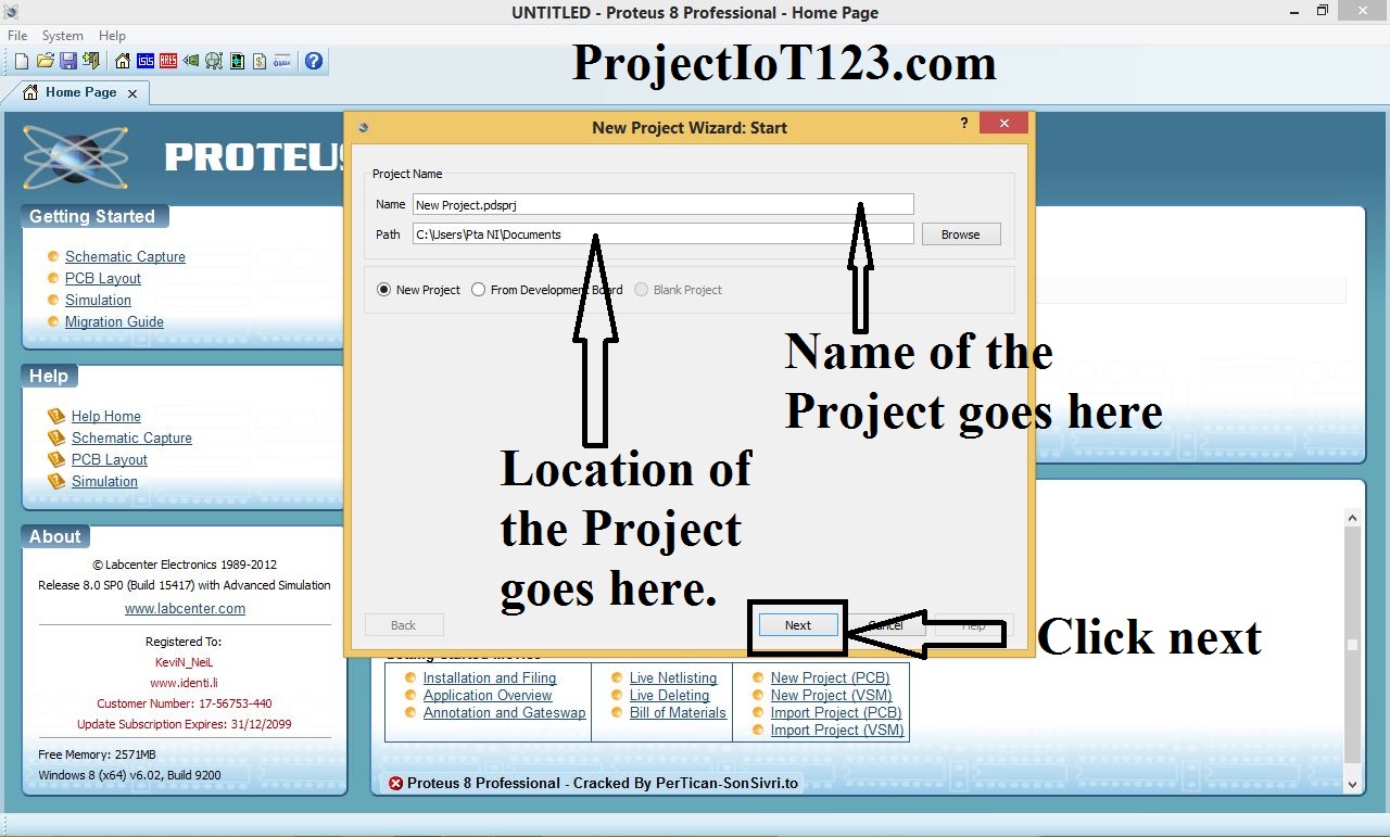 Now follow the steps as shown in the following images:
 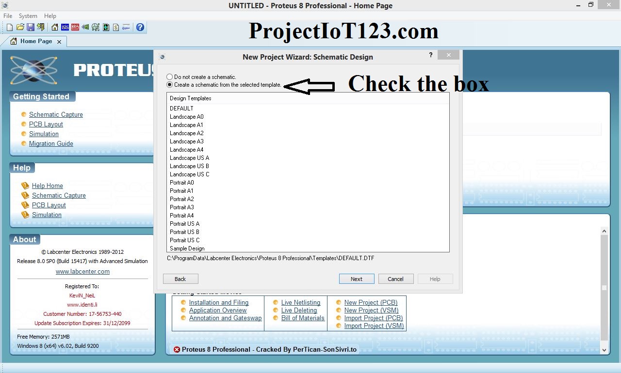 [otw_is sidebar=otw-sidebar-2]
 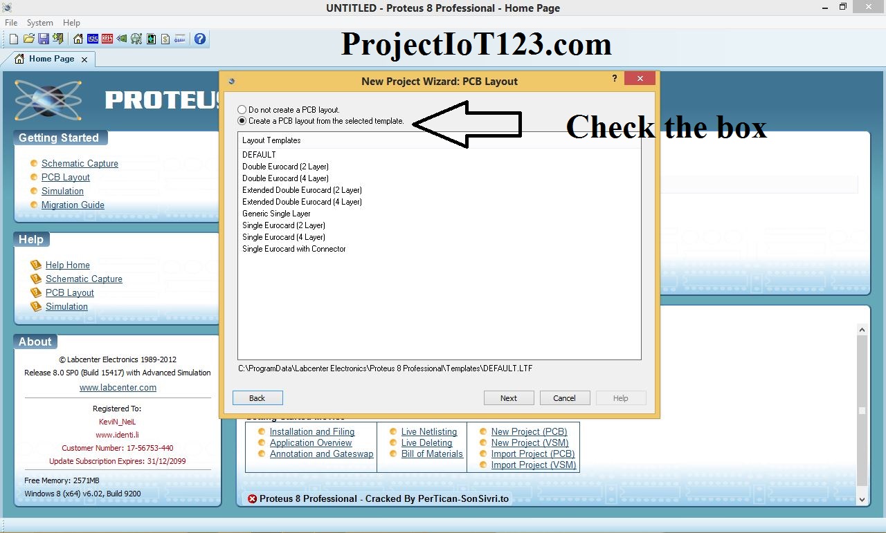 Now as shown in the following image check the circle of no firm ware as we will not be needing any for this project:
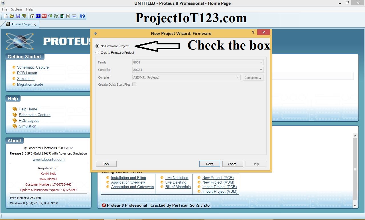
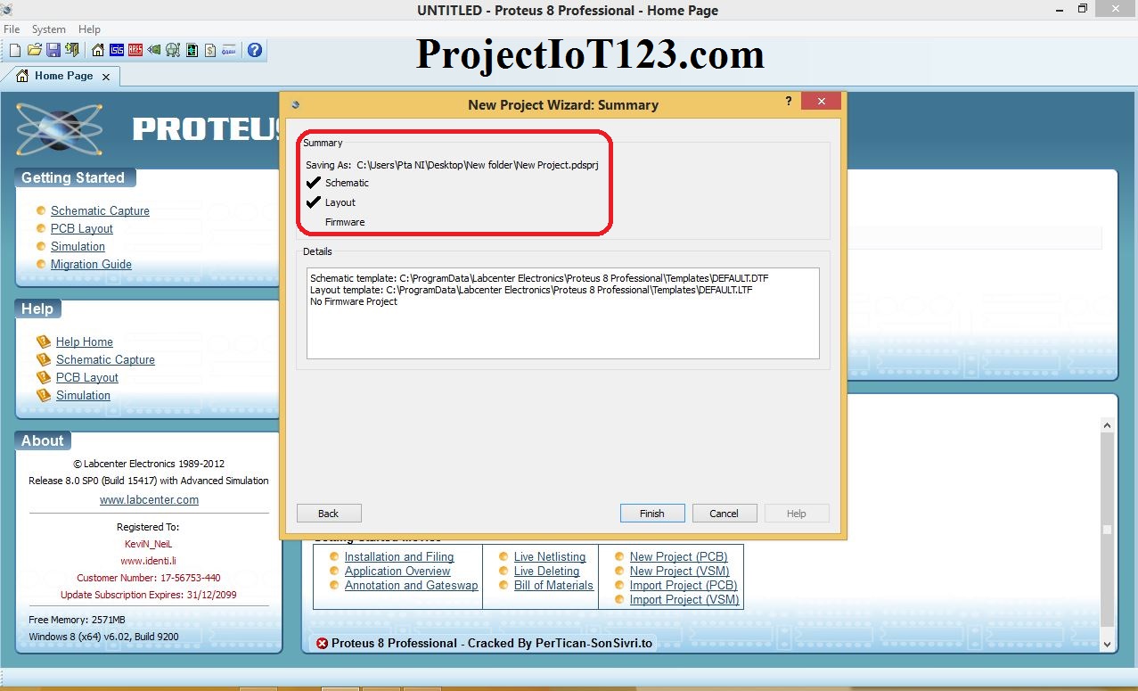 After completing all the steps you wills the dialog box as shown in the above image:
Step2:
Now let us create the schematic in the Proteus:
How to Convert Schematic to Pcb Layout in Proteus:
[otw_is sidebar=otw-sidebar-3] The circuit shown in the above image is the non-inverting amplifier circuit and is drawn using the Proteus schematics capture tool. 
Step3:
Now let us come on to the side of the PCB layout. In order to design the printed circuit board we first need to specify the board dimension of the PCB Design in Proteus. The Board dimension can easily be specified as shown in the following image: 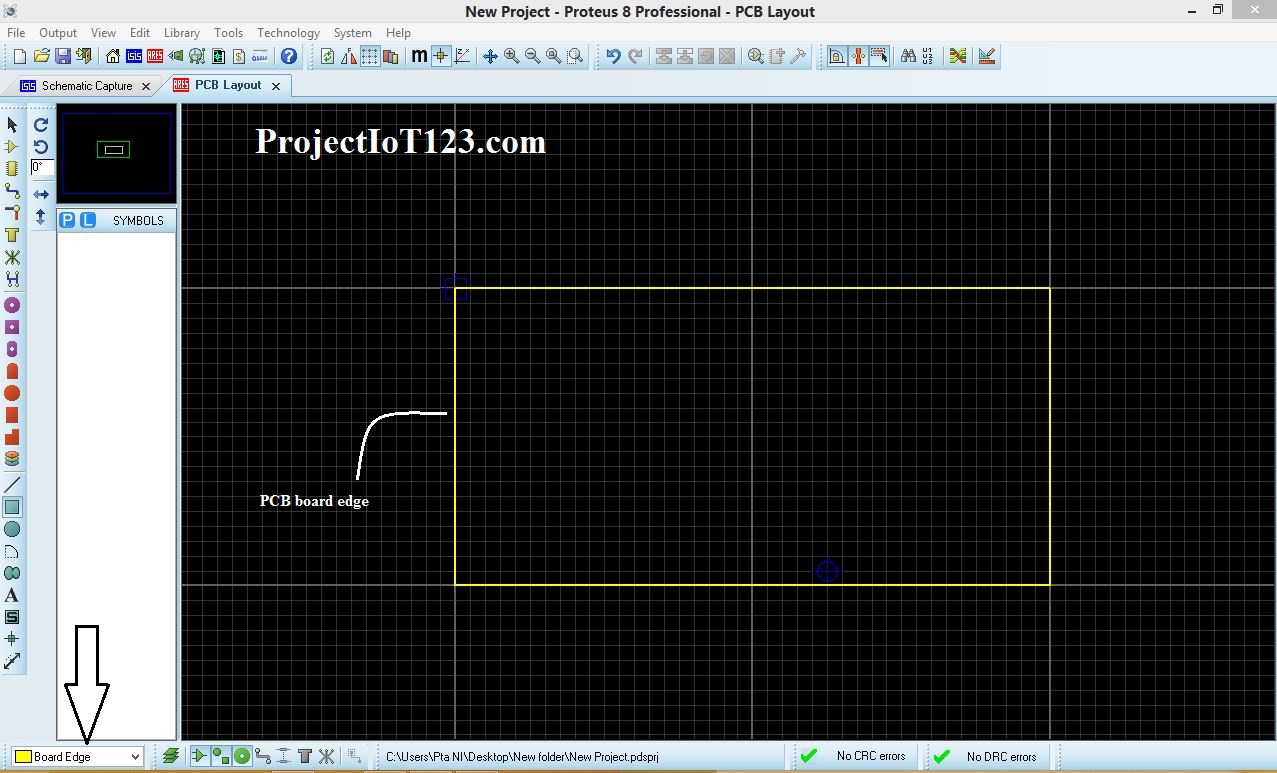
Step4:
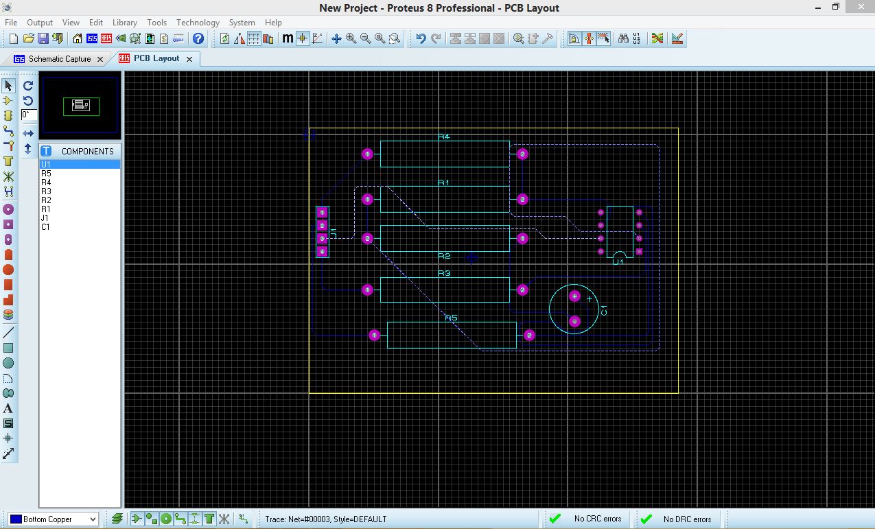
After we have specified the board size of the printed circuit board let us place all the components of the schematics onto the board. The board will look like the following after placing all the components: 
Step5 how to print pcb layout from proteus:
Now let us route the PCB design. Routing means that the copper traces would be lain on the printed circuit board in order to provide the circuit connectivity. The board will look like the one in the following image after routing the printed circuit board: [otw_is sidebar=otw-sidebar-2]
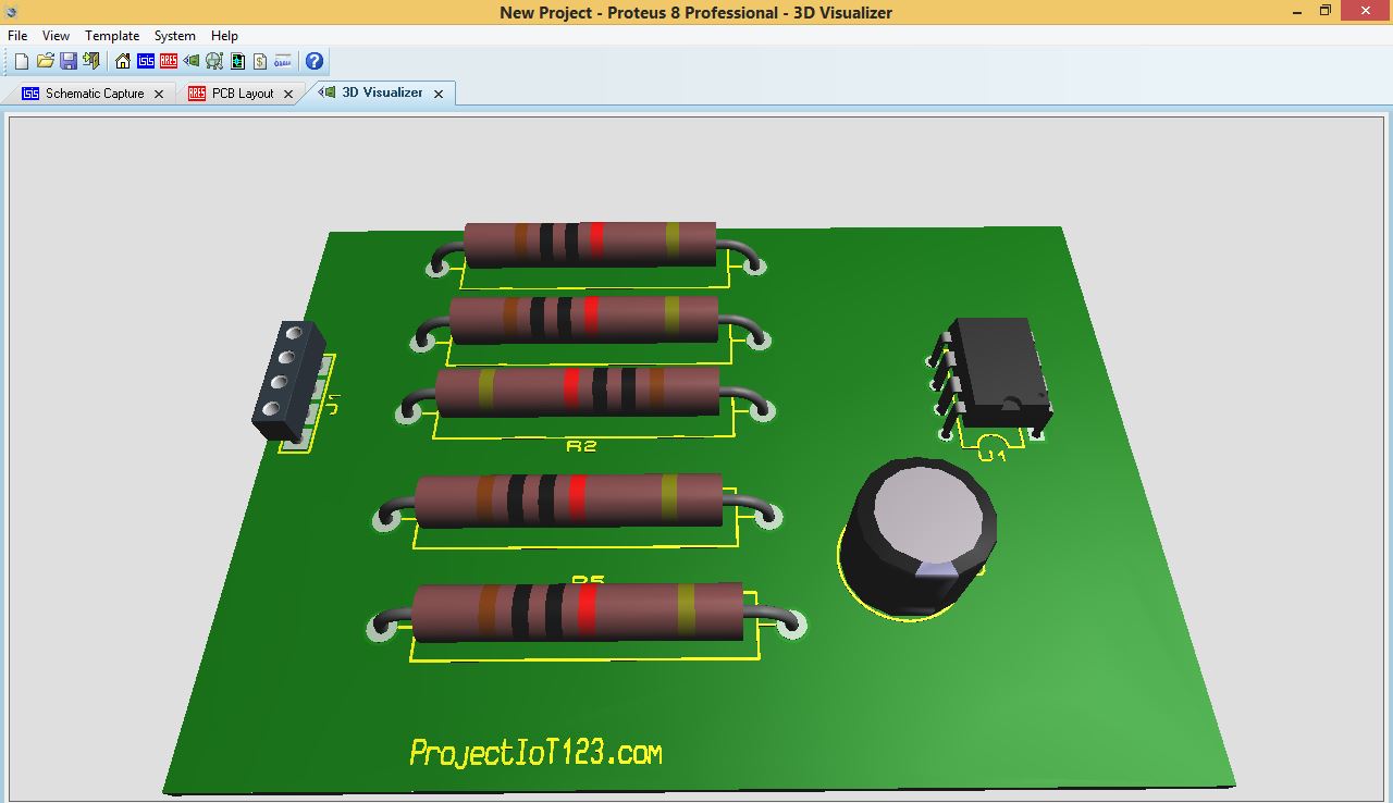
 The traces in blue denotes that the copper is lain below the printed circuit and our PCB is one sided. Step6: Now I will visualize the three dimension view of the circuit. The three dimensional view of the printed circuit board that we have designed looks like the one in the following image: [otw_is sidebar=otw-sidebar-1]
Orcad Allegro Tutorial for Beginner
This tutorial will present the Orcad Allegro Tutorial for Beginner, in this tutorial I will discuss about the basic tools of the Allegro PCB designer. That is all for now. I hope this post would be helpful for you. In the next post I will come up with more interesting applications of Proteus and educational topics. Till then stay connected, keep reading and enjoy learning.
Eagle Pcb Design Software Tutorial
STEP BY STEP EAGLE PCB DESIGN SOFTWARE TUTORIAL
https://projectiot123.com/2020/01/24/eagle-pcb-design-software-tutorial/ [otw_is sidebar=otw-sidebar-3]
Hello sir/madame,
This is Park from Quint Tech,our company has over 10 years experience in manufacturing in PCB and PCBA market.
We have a professional purchasing team to help us supply the components with good price and quality to our customers.
And the parts are original, the quality is guaranteed.
Our advantages are as below:
1. Fast delivery: 2-3 days for 1-4 layers boards,aluminum boards.
2. Competitve price: we can help to save at least 10-15% cost for you.
3. Guaranteed quality: we have a strong purchasing team and supply chain,complaint rate less than 1%.
If there is any PCB or PCBA project that i can quote for you,please feel free to contact me.
Best Regards
Park Zhao
Our mission:
To be your satisfactory one-stop PCBA manufacturing service expert
QUINT TECH HONGKONG LIMITED
Add: Room 903,Block B,TengYao Building,No.268,
GuShu 2nd Road,XiXiang Township,BaoAn District,
Shenzhen 518102,P.R.China
Tel: +86-755-2359 2155
FAX: +86-755-8321-6066
Email: sales@quint-tech.com
Web: http://www.quint-tech.com
Тревожитесь за местонахождение ваших детей или важных вам людей? Наш сервис определения местоположения по номеру телефона дает точный ответ на ваш вопрос.
Наш сервис гарантирует быстрое и точное определение местоположения. Это ваш надежный инструмент для поддержания связи и безопасности.
Ваша конфиденциальность – наш приоритет, поэтому мы используем только легальные способы слежения.
Не позволяйте случайностям управлять вашей жизнью. Выберите наш сервис и действуйте с уверенностью.
[url=https://taplink.cc/poisk_telefona_po_nomeru]Поиск местоположения человека по номеру телефона[/url]