
cadence allegro pcb designer tutorial 31
[otw_is sidebar=otw-sidebar-1]Hey guys! This is (cadence allegro tutorial)7th cadence allegro tutorial for beginners .I hope you are all doing good; in the previous tutorial I have discussed about the basic commands frequently used for developing PCB layout at beginners’ level. Allegro PCB Designer is an important software for PCB designing used by professionals so basic understanding of the software is crucial.
Introduction to Allegro PCB Designer (PCB Stack-up and Visibility Window: Part 7)
In this tutorial I will discuss about the “Visibility” window and PCB layers, in my previous tutorials I have discussed about the “Options” and “Find” windows, so “Visibility” window is another window besides these two windows and also used frequently while designing the PCB layout. Let us first discuss the PCB layers and PCB stack-up.
Note:
Cadence Allegro Tutorials
| LIST OF Cadence AllegroTurorials | Names |
| Tutorial # 1 | Introduction to Allegro PCB Designer |
| Tutorial # 2 | Allegro Use “Add Connect Tool” |
| Tutorial # 3 | Allegro Use “Slide Tool” |
| Tutorial # 4 | Allegro Use “Hilight & Dehilight Tool” |
| Tutorial # 5 | Allegro Use “Show Measure & Grid” |
| Tutorial # 6 | Introcution to Nets in Allegro |
| Tutoiral # 7 | Introcution to Stackup in Allegro |
| Tutorial # 8 | Introcution to Copper Shapes in Allegro |
| Tutorial # 9 | Introduction Vias and GND Plane in Allegro |
ALL Orcad Allegro Tutorial for Beginner Ask free to Question us
PCB Layer Stack-up:
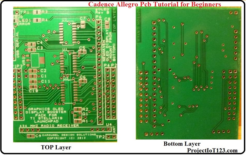
If you are studying engineering you might have seen the circuit assembled on the printed circuit board. A simple circuit is fabricated on a single layer of the PCB only that is all the electronic components are placed on one side of the PCB and routing is done on the other side. Another important thing is that all electronic components employed are through-hole package. A single layer PCB is shown in the following image:
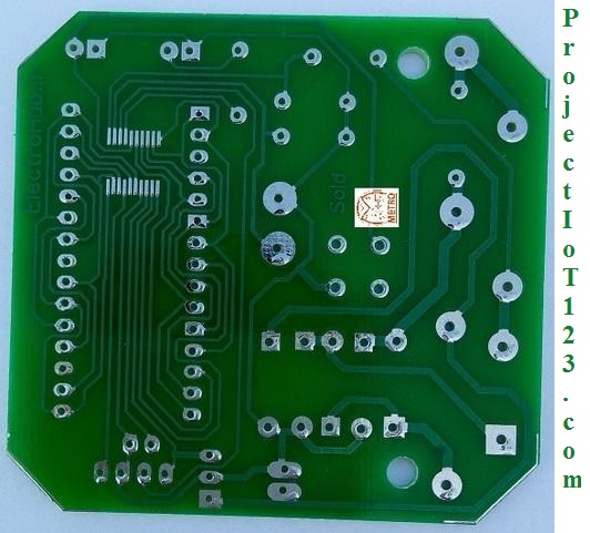 However there are some situations when routing and component placements is to be done on both sides of the PCB. That PCB will be called “Two layer PCB” or “Double Layer PCB”. “Two Layer PCB” is as shown as shown in the following image:
On a two layer PCB more components can be placed and more routing can be done. Similarly there are three layer and four layer PCBs. The number of layers on the PCB is determined by the PCB designer according to circuit complexity.
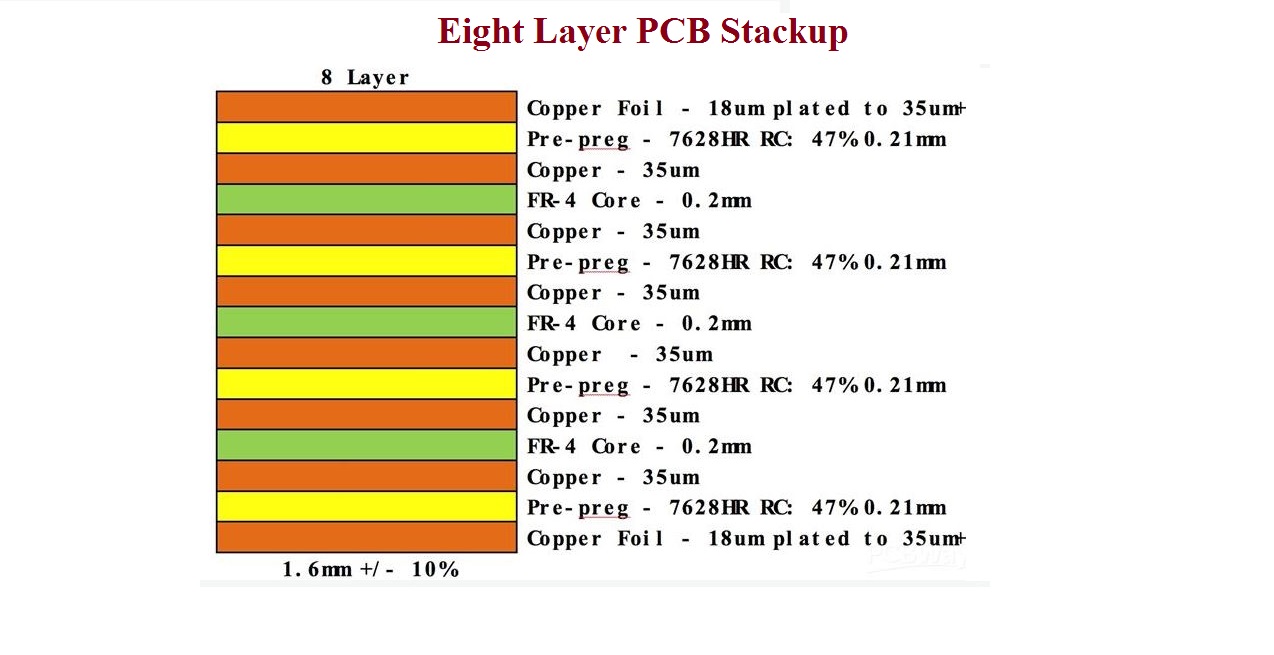
The PCB layer stack-up is defined as the combination of copper layers and insulation layers on the printed circuit board. Eight layer PCB stack-up is as shown in the following image:
The following image shows the layout design of two layer PCB. The top side of the PCB is represented by the Blue colour and the Bottom side is represented by the pink colour.
Let us now discuss the “Visibility” window.
Visibility Window:
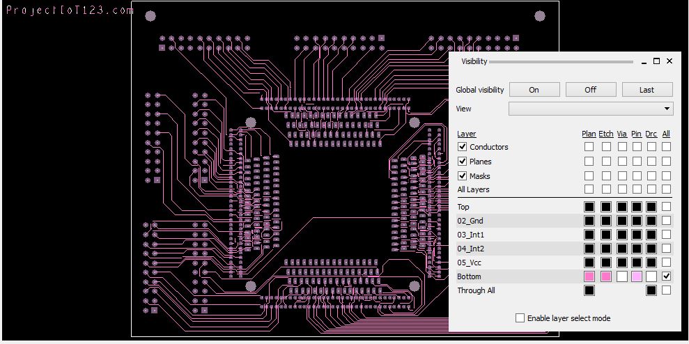
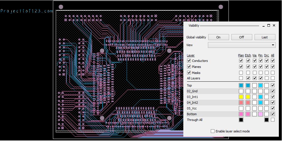
The “Visibility” window is the third and last window that is shown at the extreme right side of the GUI of the Allegro PCB Designer along with “Options” and “Find” window. These two windows are of vital importance while working with commands, I have discussed in detail about the “Options” and “Find” windows in my previous tutorials. It is recommended to go through my previous tutorial in order learn about the two windows. The visibility window is as shown in the following image:
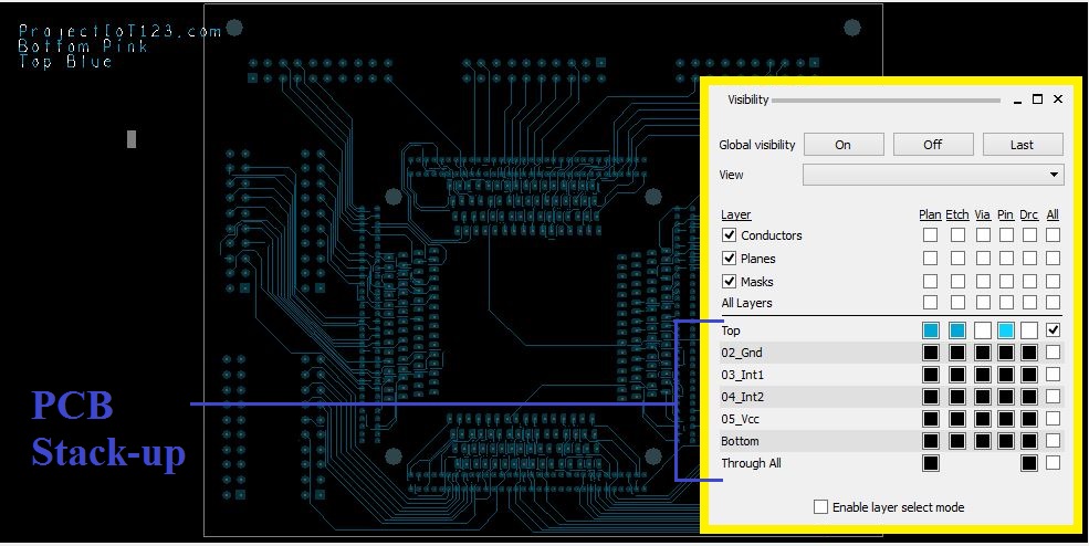 In the “Visibility” window the PCB stack-up is shown as represented in the above image. The PCB is six layer as can be seen in the stack-up. The six layers shown are:
- Top.
- GND
- _Int1
- Int.
- _Vcc.
- Bottom.
Only the check box of the “Top Layer” is checked so only top layer is visible as shown in the blue colour. The following figure shows the Bottom layer checked and all other layers left unchecked so only bottom layer is visible.
In the cadence allegro tutorial following image all the layers are tuned visible by checking the check box of all the layers.
At this point most of you might be thinking that how the connection between the top, bottom and other layers are established. The answer to this question is “vias”. “Via” can be thought of as the metallic rod which penetrates through the PCB and enables the connection between the layers. The route (copper) that needs to be connected from top to bottom layer is connected to the “via” which is also attached to the copper etch at the bottom. The detailed discussion on the “Vias” will follow in the next tutorial.
That is all for now, I hope this tutorial(cadence allegro tutorial) would be helpful for you. In the next tutorial I will discuss other basic commands. Till then stay connected, keep reading and enjoy learning.