
Introduction Vias and GND Plane PCB 1
[otw_is sidebar=otw-sidebar-1]I hope you all good, this is the ninth part in series of tutorials on “Introduction to Allegro PCB Designer”. In the previous tutorial I have discussed about the basic commands used frequently for designing layout at beginners’ level. I have also discussed about the crucial techniques that are to be considered for optimizing the layout.
Introduction to Allegro PCB Designer (GND plane, Vias and Fanout)
In this tutorial I will discuss other basic commands and I will also explain other techniques for efficiently developing the layout of the PCB. I will discuss about GND plane, how to use vias and procedure of fanout in the PCB.
Note:
Cadence Allegro Turorials
| LIST OF Cadence AllegroTutorials | Names |
| Tutorial # 1 | Introduction to Allegro PCB Designer |
| Tutorial # 2 | Allegro Use “Add Connect Tool” |
| Tutorial # 3 | Allegro Use “Slide Tool” |
| Tutorial # 4 | Allegro Use “Hilight & Dehilight Tool” |
| Tutorial # 5 | Allegro Use “Show Measure & Grid” |
| Tutorial # 6 | Introcution to Nets in Allegro |
| Tutoiral # 7 | Introcution to Stackup in Allegro |
| Tutorial # 8 | Introcution to Copper Shapes in Allegro |
| Tutorial # 9 | Introduction Vias and GND Plane in Allegro |
[otw_is sidebar=otw-sidebar-2]
ALL Orcad Allegro Tutorial for Beginner Ask free to Question us
GND Plane PCB:
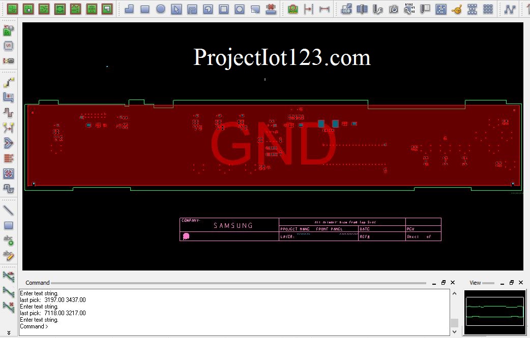
In the previous tutorials I have explained that in order to connect the power pins together copper shapes are employed instead of ordinary Clines as the power pins dissipates more power as compare to data signals. In the same way the GND pins need also be connected together with copper shapes. The copper shape that is used to connect the GND pins is usually called the GND plane. In the situations where we have a multi-layer printed circuit board we can select any layer to lay copper shape for GND and connect all the GND pins to that layer with the help of the via. In the situations where we have only single layer copper shape for ground plane is added on the same layer. The following figure shows the GND plane in multi-layer board.
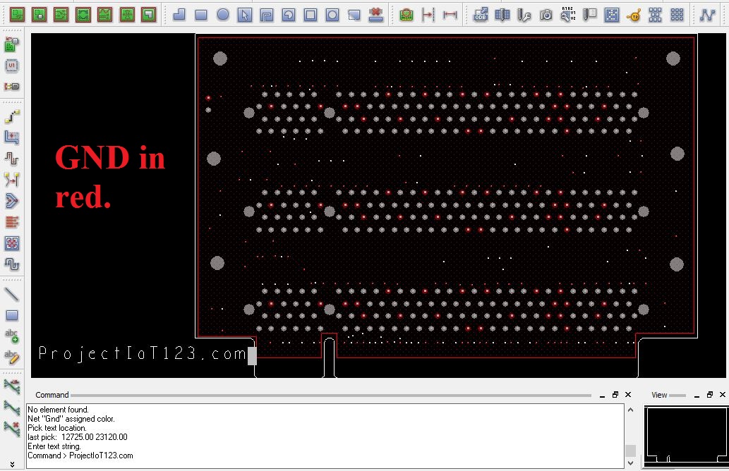
The following figure shows the GND plane on the single layer PCB.
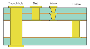
In order to connect the GND pins of the components that are placed on top and bottom of the PCB to the GND plane that is in between the PCB via is used. Via establishes the connection between different layers of the board. The following figure shows the application of via in order to connect GND pins to the GND layer.
Let us now see how to add via in the PCB.
Via:
As explained earlier that via can be considered as the metallic rod that establishes the connection between different layers. The placement of the via is simple, first click on the icon of the “Add Connect” command and then select the pins to which the via is to be attached. Drag the cursor to create little Cline and then double click to place the via. When the via is placed the connection will automatically be created. The visualization of the via can be achieved from the following image:
[otw_is sidebar=otw-sidebar-3]
Fanout:
Let us now learn about the Fanout. Fanout is the process which is deployed while working with the multilayer PCBs. When the high speed signals are to be routed or when the signal grounds are to be connected to GND plane, the vias are connected to the pins with Clines as short as possible. The following figure shows that the PCI (Peripheral Connect Interface) signals and signal ground are fanout:

That is all for now, I hope this tutorial would be helpful for. In the next tutorial I will discuss other basic commands in detail that are frequently for developing the layout of the PCBs. Till then stay connected, keep reading and enjoy learning.